

Debasis Mohapatra
Bengaluru, 1 November 2026
Odisha is likely to emerge as a major semi-conductor hub in coming years as the eastern state of India is currently executing five semi-conductor projects worth $4 billion.
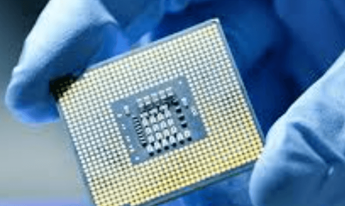
These new projects are coming up in semiconductor fabrication and advanced 3D chip packaging among others.
According to Vishal Kumar Dev, Additional Chief Secretary (ACS) of the Electronics and Information Technology Department of Odisha govt, two of the 12 projects approved under India Semiconductor Mission is coming up in the state.
Currently, India’s first compound semiconductor fabrication unit and first advanced 3D chip packaging unit are under construction, as per the senior govt official.
Upcoming projects:
SICSem: India’s first commercial Silicon Carbide (SiC) compound semiconductor fabrication unit, approved under the India Semiconductor Mission with a capacity for 60,000 wafers is coming up in Odisha’s capital, Bhubaneswar. The project, which is coming up at an investment of around $230 million, is expected to be fully operational by 2027-28.
3D Semiconductor Packaging Project: Odisha govt has entered into agreement with chip maker, Intel & US-based 3D Glass Solutions to build an advanced semiconductor packaging & glass-core substrate manufacturing facility. This is India’s one of the most advanced tech investments in the semiconductor space, which will see an investment of more than $3 billion and is likely to be operational around 2028.
Silicon Carbide Substrate Wafer Facility: QuadQuantum has signed a Letter of Intent (LoI) with the Odisha govt to establish a silicon carbide (SiC) substrate wafer facility in the state. Details of the investment and time period are yet to be revealed by the state.
Apart from these, Odisha govt is setting up an Integrated Power Electronics Hub at an investment of Rs 452 crore at IIT, Bhubaneswar. The state is also developing ‘Odisha Silicon Valley’ at Cuttack.