


R Prasad
Bhubaneswar, 3 September 2025
It is a pride moment for Odisha. The state finds a place in the first ‘Made in India’ chip initiative. Three semiconductors have been unveiled at Semicon India-2025 ceremony held at Yashobhumi, New Delhi on Tuesday.
On this occasion the Electronics and IT minister of Govt of India, Aswini Vaishnaw presented Prime Minister Narendra Modi with 32 India-made chips, out of which 3 are from Odisha.
Two semiconductors are designed by NIT, Rourkela and one by Parala Maharaja Engineering College of Berhampur. NIT, Rourkela designed VG Amplifier and Sesor Circuit-C2S0018 and the Present Encryption Core-C2S0017. Similarly PMEC developed high performance multiplier IC-C2S0061.
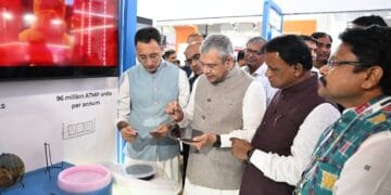
On this event Odisha Chief Minister Mohan Charan Majhi, IT minister of Odisha Mukesh Mahaling, Chief Secretary Manoj Ahuja, Prinipal Secretary of IT, Odisha Vishal Deb and other high-ranking officials attended the event. CM Majhi also inaugurated the Odisha Pavillion.
In a post on social media x, CM Majhi said it is a matter of immense pride for Odisha to be part of first Made In India chip initiative. These remarkable achievements showcase the talent and innovation nurtured within our state and highlight Odisha’s growing role in India’s semiconductor journey. I warmly congratulate everyone associated with these historic milestones, which represent significant steps towards technological leadership and reflect the unwavering commitment of our institutions to research, innovation and self-reliance.
Recently, union cabinet approved 4 semiconductor manufacturing plants for the country, out of which two are for Odisha worth Rs. 4009 cr. The two projects will be set up at Info Valley of Bhubaneswar by SICSem and 3D Glass.
SICSem Pvt. Ltd, in collaboration with UK-based Clas-SiC Wager Fab Ltd. will set up India’s first commercial compound semiconductor fabrication facility. The Plant will manufacture silicon carbide (SiC) devices, known for their efficieny in high-power applications, with an annual capacity of 60,000 wafers and 96 million packaged units.
The US-headquartered 3D Glass Solutions Inc (3GDS) will introduce the world’s most advanced semiconductor packaging technology. The unit will manufacture glass interposers, silicon bridges and 3D heterogeneous integration (3DHI) modules. With a planned capacity of about 69,600 glass panel substrates, 50 million assembled units and 13,200 3DHI modules annually, the facility will cater to applications in defence, high performance computing, artificial intelligence, RF and automotive electronics, photonics and co-packaged optics. The two projects will bring cutting-edge technogy to Odisha, official said.


